ADI reveals next generation for MEMS switches for test
lanka 2020-11-20 14:42:58
Analog Devices revealed details of its second generation of micromachined electro-mechanical relays for automated test.
The aim is to provide an alternative to relays – which have good DC performance and poor RF performance – and semiconductor switches – which have poor DC performance and good RF performance – in a single device with good DC and good RF performance – ADI is claiming 34GHz operation.
Given good RF and DC characteristics, both a power tester and RF instruments can be connected to a terminal of a unit-under-test through a cluster of identical switches. Generic loop-back testing is another potential application.
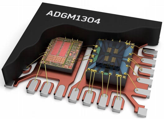 Several years ago ADI introduced its first generation of MEMS relays, typified by the ADGM1304 (left).
The MEMs switch in these is a cantilever with a contact on the end which is pulled down to complete a circuit by bending the cantilever using electrostatic force. In the diagram are four switches on the MEMS die, which is co-packaged with a high-voltage chip that provides ‘gate’ drive for the cantilevers.
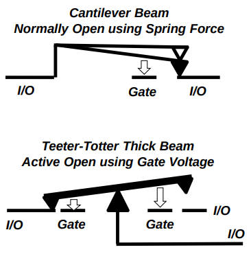 For generation 2, the company has gone away from a cantilever and adopted a see-saw movement operated by two gate electrodes (schematic right) which has at least three advantages:
Firstly, on and off times are now balanced – at ~30μs each, and secondly there is a option to do change-over switching instead of only SPST switching. The third is more subtle – if kept operated, the cantilever in gen1 would gradually bend and eventually stay closed when the drive voltage was removed – leading to a ‘max constantly on lifetime’ specification being introduced – seven years in the case of gen1, which is now >10 years in gen2.
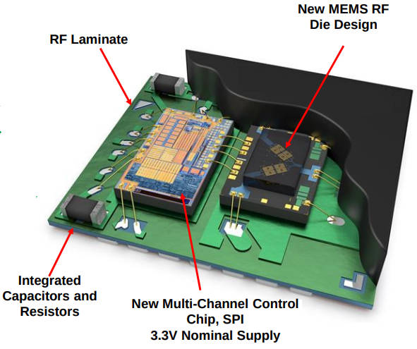
80V is needed to electrostatically create generate sufficient operating force, once again provided by a co-packaged IC (diag top right). The package is 4 x 5 x 0.95mm.
The new integrated driver chip can also now offer an SPI serial interface – compared with the parallel interface of the first generation, and there has been a move to an internal circuit board (which was a lead-frame in gen1) to allow passive components to be integrated, including decoupling capacitors and 10MΩ resistors on the contact ports – the latter to drain away charge build-up on any connected parasitic capacitance to prevent high (damaging) current surges when the contacts close.
The driver chip needs 3.3V at 2-3mA to turn a contact on.
 Physically, the see-saws and contacts are gold, built in a back-end process after support frames are etched from high-resistivity silicon in a CMOS fab.
Specs for the contacts (drawn left) include 3Ω contact resistance, ±6V maximum make and break voltage, ±20V open withstanding voltage, 200mA continuous current and 16fF open-circuit capacitance.
RF-wise, -10dBm can be switched into 50Ω without reducing lifetime from its purely mechanical switching lifetime, and 33dBm can be handled.
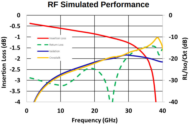 Adding the internal circuit board has also allowed internal circuit paths to be improved by turning them into transmission lines. A summary of RF specs is available in the graph (right). A highlight here according to ADI apps manager Eric Carty is a 1.5dB insertion loss at 34GHz.
Linearity is 69dBm and isolation is around -20dB.
With SPDT switches and space for passive components on the board, will ADI be making non-reflective switches?
“We could do them,” is all Carty was prepared to say at the time, when ADI spoke to Electronics Weekly during virtual Electronica.