Lattice picks FD-SOI and redesigns FPGAs for embedded vision and edge AI
lanka 2020-11-06 10:27:28
Lattice has switched to 28nm FD-SOI (fully-depleted silicon-on-insulator) technology for a range of sram-based FPGAs intended for embedded vision and artificial intelligence processing in industrial, automotive and consumer systems.
Although they are ram-based, and therefore need to boot from adjacent memory, the firm has found a way to get chip outputs enabled, set and stable within 3ms of power-up – allowing the FPGAs to be used where false output states must be avoided, such as in motor control, instead of traditionally faster-starting flash-based FPGAs.
Called CrossLink-NX, the family “was designed using the new Lattice Nexus platform, which combines a 28nm FD-SOI manufacturing process with a new Lattice-designed FPGA fabric architecture optimised for low power operation in a small form factor”, according to the firm.
“It is also supported by a library of design software, IP blocks and application reference designs,” said Lattice director of marketing Gordon Hands. “These make it quick for developers to integrate CrossLink-NX FPGAs into new or existing Edge designs.”
Amongst architectural changes compared with its earlier offerings, and particularly for AI processing, the firm has increased memory ratio to 170bit/logic cell – adding 0.5Mbit blocks of memory alongside the 18kbit blocks it introduced a while ago, and its traditional distributed memory.
High-speed hardened (non-FPGA), and fast programmable IO, including MIPI, PCIe and DDR3 for memory, has been included to suit embedded vision applications.
Hardened
- 8 D-PHY lanes at 2.5Gbit/s
- one PCIe lane at 5Gbit/s
Fast programmable
- up to 12 MIPI D-PHY at 1.5Gbit/s
- LVDS, subLVDS, SGMII
- DDR3 at 1,066Mbit/s
- up to 192 IOs total
Alongside the IO and memory are DSP blocks and either 17,000 or 40,000 logic cells (LUT4 type)) depending on device (see table).
 Initial parts are CrossLink-NX-17 and -40
Lattice is emphasising the small minimum package size
*available at launch
The 28nm FD-SOI process was chosen after “we spoke to hundreds of different product design groups” according to Hands, which revealed the most common uses were likeley to be in 5G comms, embedded vision, safety-critical, smart home, smart factory and cloud-based platforms.
The switch to FD-SOI – made in Samsung’s fabs – automatically brings lowered power consumption through reduced parasitic capacitance, as well as two other advantages.
The first is that whole-chip electric field control is available through substrate biasing (‘back-biasing’) – allowing device speed to be traded off for power consumption. According to Hands, this is used during product manufacture, and is available to users (although not on-the-fly – device configuration must be re-loaded after a bias change).
Second comes much-reduced soft error rate, because alpha particle and gamma ray events in the underlying substrate can no longer affect transistor channels (see diagram). “Soft error rate is up to 100 times lower than in similar FPGAs, making it a compelling solution for mission critical applications that must operate safely and reliably. The initial CrossLink-NX device is designed to support ruggedised environments found in outdoor, industrial and automotive applications,” according to Lattice, which is claiming 21.84 FIT (failures in time over 1bn hours).
 Compared to bulk silicon ICs, FD-SOI chips have far less volume (orange) vulnerable to soft errors
Low power consumption is claimed, at <40mW worst case in an 100kHz 85°C application and 75mW in a different 200MHz application.
To give some idea of capability, the 40k cell version will be capable of both video bridging and video processing, said Hands, adding that it could support multiple displays.
Fast boot-up comes from using quad SPI memories running at up to 150MHz as non-volatile configuration storage.
Hands explained that, after speaking to five SPI memory vendors, Lattice developed a power-up polling scheme that interrogates the ‘SFDP’ (serial flash discoverable parameter) tables in the memory. “We are utilising the capability around SFDP to determine whether the SPI memory is ready to be used or not,” he said. The FPGA then loads and acts on IO configuration data first – hence the 3ms to stable IO – and then loads the rest of the configuration to get the whole FPGA functioning as programmed less than 15ms from power-up, he claims.
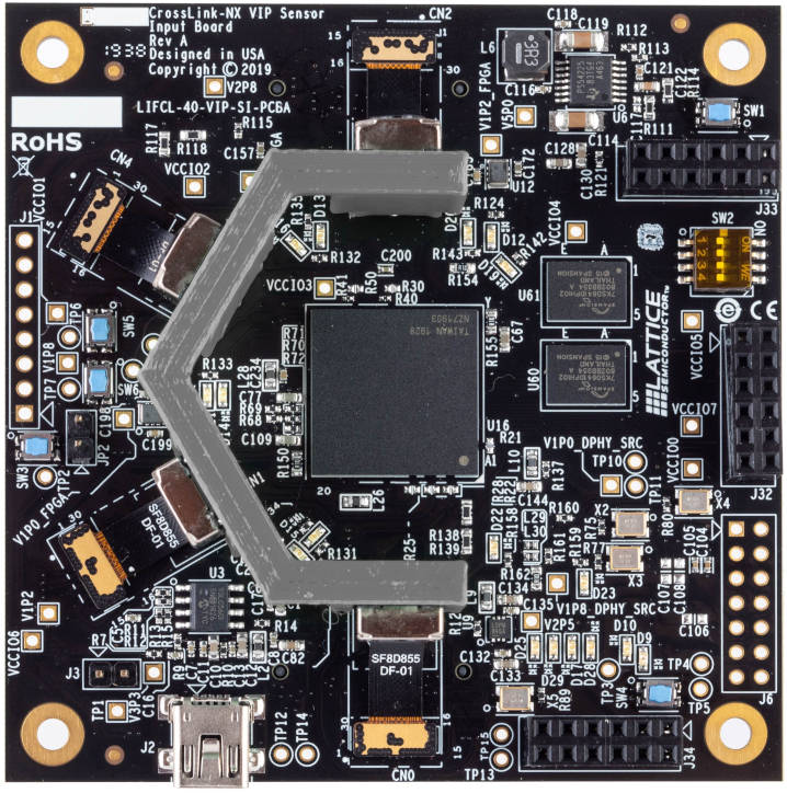 Sensor development board for CrossLink-NX
To go along with its Nexus devices, Lattice has updated its Radiant design tool to version 2.0. “In addition to adding support for higher density devices like the CrossLink-NX FPGA family, the updated design tool also offers new features that make it faster and easier than to develop Lattice FPGA-based designs,” according to the firm.
“Developers with little to no experience working with FPGAs should be able to quickly leverage the automated features of Lattice Radiant,” claimed product line manager Roger Do. “The tool leads them through the design flow from design creation, to importing IP, to implementation, to bit-stream generation, to downloading the bit-stream onto an FPGA.”
For experienced FPGA developers, he added, v2.0 allows for more granular control over FPGA settings if specific optimisations are required.
Added features include:
- On-chip debugging tool for bug fixing in real time – virtual switches or LEDs can be inserted into code to confirm viability. Hard IP block settings can be changed.
- Improved timing analysis for more accurate trace-and-route planning and clock timing to avoid design congestion and thermal issues.
- Engineering change order (ECO) editor now allows incremental changes to a design without having to recompile the entire FPGA database.
- ‘Simultaneous switching output’ (SSO) calculator analyses individual pin signal integrity in proximity to other pins.
On top of Radiant 2.0, there is a library of IP cores including MIPI D-PHY, PCIe, SGMII and OpenLDI interfaces, and demos for common embedded visions applications such as 4:1 image sensor aggregation.
For machine learning and artificial intelligence use, the firm’s SenseAI tools can be used.